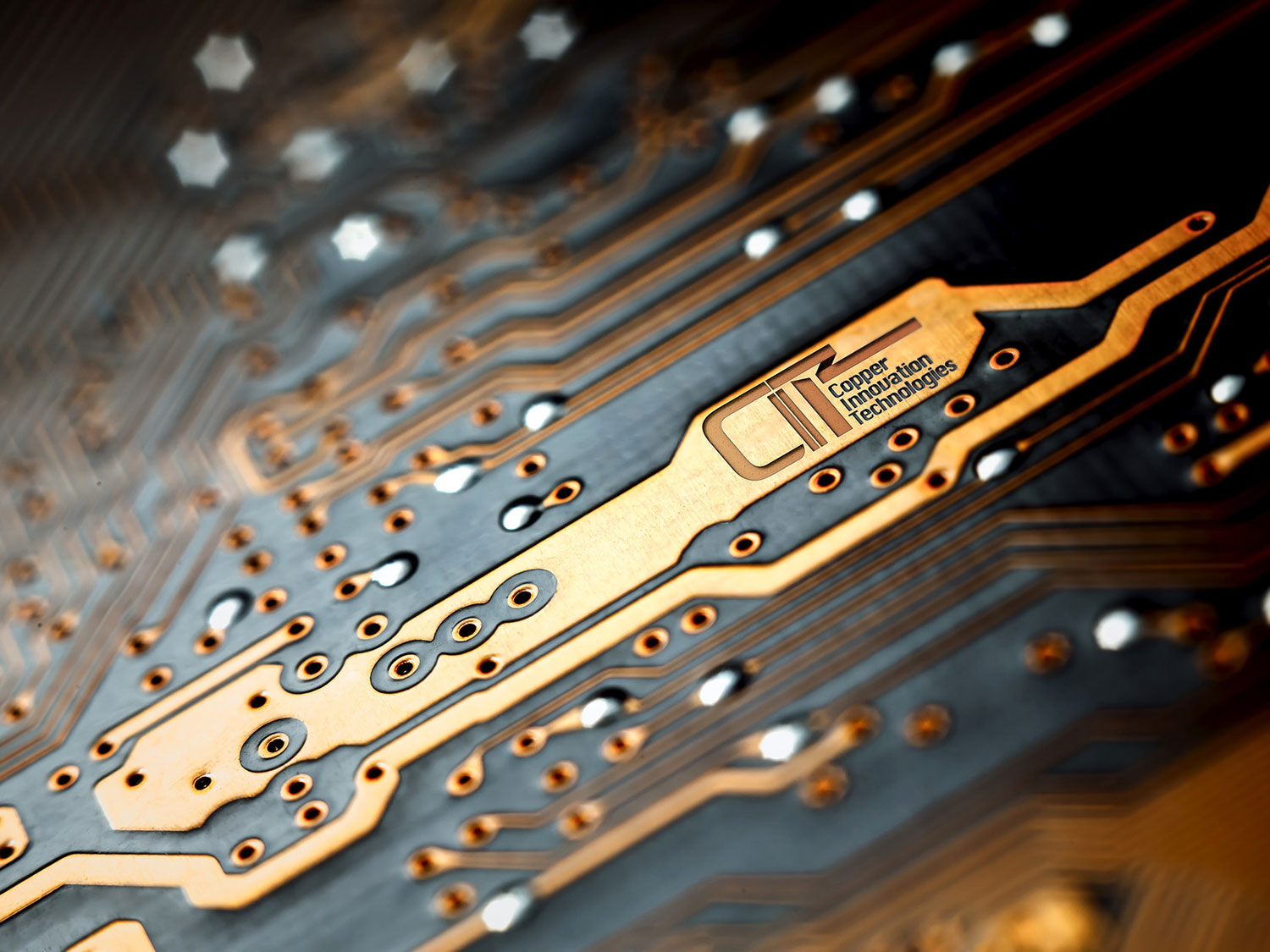

Copper Innovation Applied sciences (CIT, official site) is an organization we’ve had a possibility to speak to across the December to CES 2024 timeframe. They developed a brand new Copper-Clad Laminated Movie (FCCL) know-how to enhance digital knowledge transmission by decreasing the signal-to-noise ratio (SNR).
The FCCL precept works as comply with: a copper layer is someway bonded to a versatile substrate (plastic-looking materials). This permits the constructing of versatile printed circuit boards (PCB) with exact circuitry. In an period of versatile shows and foldable units, you possibly can think about how beneficial this know-how might be for cutting-edge electronics.
Along with the versatile nature of its FCCL know-how, CIT additionally factors out that its copper materials has a single-crystal construction, which implies that atoms are exceptionally nicely aligned, with fewer grain boundaries. This construction permits for even higher electrical and thermal conductivity as grain boundaries impede the movement of electrons, thus sustaining sign integrity (noise discount).
The decrease resistivity of this sort of copper can be essential to transmitting a sign with minimal loss and interference. That’s notably true for a weak unique sign.
The identical properties might be important for very high-speed indicators akin to 5G and 6G going ahead. Regardless of the throughput, the know-how that CIT is engaged on may drastically enhance tomorrow’s digital merchandise.
CIT began by researching methods to deposit Copper on Teflon. Alongside the way in which, the corporate developed an progressive answer that might have broader software; that’s when the corporate was based, and it’s at present positioned in Busan, however plans to develop internationally.
For instance, the corporate can construct cables with considerably lowered grain boundaries, which implies they’ll introduce as little noise as doable for analog indicators. Some indicators are very faint within the medical discipline, and it’s essential to transmit them with out introducing noise. That’s true for each “measurement” software.
CIT representatives mentioned they intend to start out addressing the electronics circuit market that makes use of Teflon, however plan to increase to extra areas later.

Depositing copper on a Teflon layer
One of many targets is to extend the deposition space dimension, which might be addressed throughout manufacturing. At present, 50x50cm is the near-term purpose to succeed in mass manufacturing actually. If all goes nicely, CIT expects to deal with most markets, from audio to medical MRI merchandise.
Most shoppers may by no means know who constructed some versatile boards inside their units, however CIT may develop into a essential participant in that market within the coming years.
Filed in . Learn extra about Korea, Semiconductors and South Korea.
Trending Merchandise